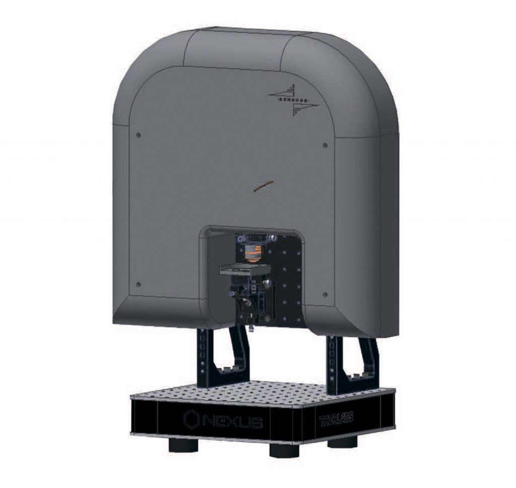
DESIGNED FOR
Non-contact measurement of the surface shape of objects in the micro- and nano- ranges of heights, altitude and step parameters of roughness, thickness of thin films, distribution of refractive index, etc.
The microscope ALLOWS you to explore reflective objects, consisting of materials that are different in their electrical properties (dielectric, conductor, etc.).
SPHERES OF APPLICATION
Biology, nanotechnology.
| Field of vision, μm | 130 × 175 |
| Altitude measurement range, μm | 0,0001 ÷ 3,0000 |
| Resolution capacity in | |
| • plane XY, μm | 0.3 |
| • by axe Z, Å | 0.8 |
| Refractive index measurement range | 1 ÷ 2 |
| Absolute measurement error of the refraction index | 1•10 -3 |
| Radiation sources | light emitting diode |
| Wave length, μm | 0.532 |
| Reconstruction algorithm | method of phase stepps |
| Image dimension, pixel | 1392 х 1040 |
| Time of measurement and processing, sec | 30 |
| Number of processed interference images | 9 |


